10+ 8255 block diagram
There are two different modes of 8255. Programmable peripheral interface 8255.
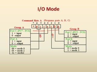
8255 Programming
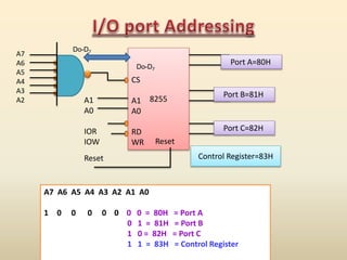
Two ports A and B function as 8-bit IO ports.

. The 8255 Pin Diagram mode 1 which supports handshaking has following features. Data busD 0 -D 7. Bit Set Reset BSR Mode.
Bit Set Reset BSR Mode. Architecture Pin Diagram Operational Modes and Control Word Format The parallel input-output port chip 8255 is also called as programmable. 8255 PPI Chip The 8255 Programmable Peripheral Interface PPI It is one of the most widely used IO chips.
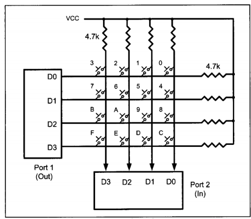
It has three separately accessible ports. A B and C The individual ports can. The 8255A is a general purpose programmable IO device designed to transfer the data from IO to interrupt IO under certain conditions as required.
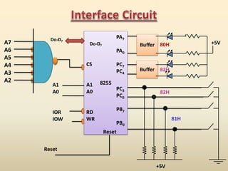
It can be used with almost any. Describe the Block diagram of 8255. Programmable Peripheral Interface Block Diagram.
These are 8 -bit bi-directional buses connected to 8085 data bus for transferring data. They can be configured either as input or output ports. The block diagram of 8255 is like this.
In this video lecture I explained about Block Diagram Internal Architecture of 8255 PPI Programmable peripheral Interface in detail In my next coming.
Atmega32 Pin Diagram Javatpoint

2019 2 3l Ecoboost Water Pump Housing Part Number Ford Mustang Ecoboost Forum
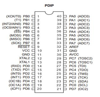
Atmega32 Pin Diagram Javatpoint
8255 Programming
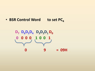
8255 Programming
Keyboard Interfacing With Avr Javatpoint
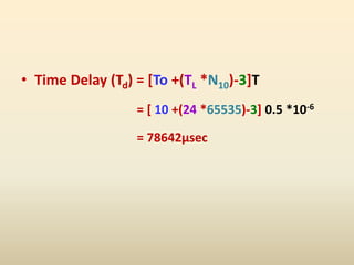
8255 Programming
Lacan S Graph Of Desire Sticker For Sale By Acidhorizon Redbubble
8255 Programming
2
8255 Programming

555 12th St Nw Washington Dc 20004 District Center Loopnet
What Is What If Analysis In Microsoft Excel Quora
The Ultimate Diagram Thread Vintage Mustang Forums
8255 Programming

Motorola 6800 Wikiwand
Qfp64 0 5 Rev2 Adapter